 |  |
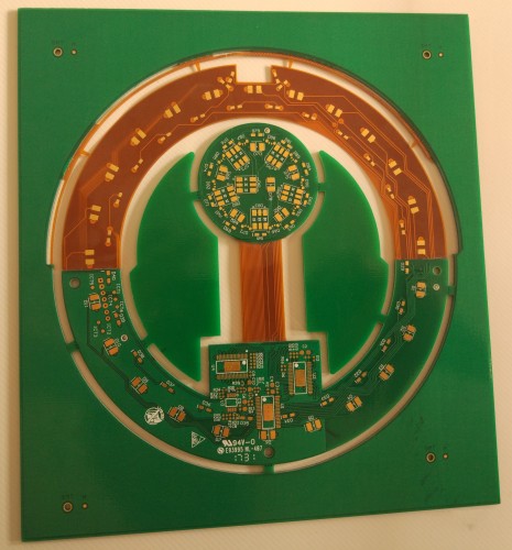
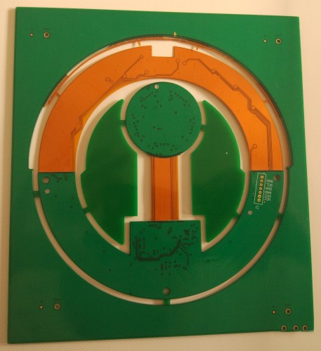
The above picture is a 6Layer Rigid-Flex PCB we made for one of our Rigid-flex PCB customers, the Rigid-Flex PCB spec is: 6layer, FR4 + PI, Rigid area 1.2mm thickness, Flex area 0.15mm thickness, Outer Copper 1oz, Inner Copper 0.5oz, Yellow Coverlay + Green Solder Mask, White silkscreen, ENIG Finish. Normally we can finish 2L Rigid-Flex PCB prototype around 12days, 4L Rigid-flex PCB prototype around 14days.
The development of FPC and PCB gave birth to a new product of Rigid-flex PCB boards (also called Flex-Rigid PCB). Flex-rigid PCB is a flexible circuit board and a rigid circuit board bonded together with laminating and other relevant technical processes. This made the Flex-rigid circuit board have both the characteristics of the FPC board and the Rigid PCB.
But Flex PCB also could add PI/FR4/SUS/Alumimum stiffeners to make some areas thicker and rigid. How to distinguish them? The main difference is the stiffeners have no any copper tracks and copper pads but only for mechnical support. And this is also the reason why Rigid-flex PCB is much more expensive than rigid PCB or Flex PCB. It's easy to make circuits on one same material, like the rigid PCB material FR4 and the flex PCB material PI. But to combind them together, it's not easy and the manufacturing processes are almost double to make the rigid-flex PCB and harder to control the PCB quality. Also rigid-flex PCB could also add stiffeners as same as flex PCB.
Advantages:
Since the Flex-rigid PCB has both the characteristics of the FPC and the characteristics of the PCB, it can be used in some products with special requirements. It has both a certain flexible area and a certain rigid area which could save the internal space, reduce the volume of finished products and improve product performance.
Disadvantages:
There are many production processes for Flex-rigid PCB, which are difficult to produce and have a low yield rate. The materials and manpower are relatively large. Therefore, the prices are relatively expensive and the production cycle is relatively long.
Rigid-flex PCB Technical Capabilities | |||
| Rigid-flex PCB Layer | |||
| NO. | ITEM | Standard Capabilities | Special Capabilities |
| 1 | Flex-Rigid PCB Layer | 2-18L | 2-24L |
| Rigid-flex PCB Material | |||
| 2 | Base Material | PI (12.5um, 25um, 50um, 100um), FR4 TG 130, 150, 170, 180 (0.05mm-3.2mm) | |
| 3 | Stiffeners | PI Stiffener: 12.5/25/50/75/100/125/150/200/250 (um) | |
| PET Stiffener: 0.125/0.188/0.25(mm) | |||
| FR4 Stiffener: 0.1mm-1.6mm | 2mm | ||
| SUS Stiffener: 0.1mm-0.5mm | |||
| Aluminum Stiffener: 0.1mm-0.5mm | |||
| 4 | EMI shielding film | HCF-6000G, PC800, etc. | |
| Board Size & Thickness | |||
| 5 | Biggest Board Size | 250mm*610mm | |
| 6 | Board Thickness | 0.6mm-5.0mm | |
| 7 | Thickness Tolerance | 0.6mm~1mm: ±0.1mm 1mm~5mm: ±10% | |
| Drill | |||
| 8 | Minimum Hole Size | 0.1 mm | |
| 9 | Holes Size Tolerance | ±0.03 mm | |
| 10 | Holes Posistion Tolerance | ±0.05 mm | |
| 11 | Minimum vias Pad Size | 0.3mm | |
| 12 | Minimum Annular Ring Size | 0.1mm | |
| 13 | Blind/Buried Vias | Yes | |
| Copper Tracks and Plating | |||
| 14 | Minimum Track Width/Space | 0.1mm/0.1mm | |
| 15 | Track Width Tolerance | 20% | |
| 16 | Tracks/Pads Position Tolerance | ≥0.06 mm | |
| 17 | Tracks/Pads To Board Edge | ≥0.15 mm | |
| 18 | Golden Finger Pitch Tolerance | Pitch:10~20mm : ± 0.03mm, Pitch:20~50mm : ± 0.05mm | |
| 19 | Copper Plating Thickness | 20-35um | |
| 20 | Hole Copper Thickness | 20-35um | |
| Surface Finish | |||
| 21 | ENIG | AU: 1-2u" Thickness NI: 40-120u" Thickness | 3u” Thickness |
| 22 | Electrolytic Nickel Gold (Hard Gold Plating) | AU: 1-50u” Thickness NI: 80-320u" Thickness | |
| 23 | Immersion Silver | Ag: 6-12u" Thickness | |
| 24 | OSP | 8-16u" Thickness | |
| 25 | Immersion Tin | SN: 10-60u" Thickness | |
| 26 | Tin Plating | SN: 5-30um Thickness | |
| 27 | ENEPIG | Au:1-4u" Thickness NI: 120-200u" Thickness Pd:1-6u" Thickness | |
| Coverlay | |||
| 28 | Coverlay Opening Size Tolerance | ±0.1 mm | ±0.03 mm |
| 29 | Minimum Drilling Size on Coverlay Opening | 0.45mm | 0.2mm |
| 30 | Minimum Square Size on Coverlay Opening | 0.7mm*0.7mm | 0.2mm*0.2mm |
| 31 | Coverlay Opening Position Tolerance | ±0.1 mm | ±0.03 mm |
| 32 | Coverlay Align Tolerance | ±0.1 mm | ±0.02 mm |
| 33 | Excessive Glue | ≤0.15 mm | |
| 34 | Minimum Area of Excessive Glue | ≤20% Pads Area | |
| Solder Mask and Silkscreen | |||
| 35 | Solder Mask Thickness | 15um +/-5um | |
| 36 | Solder Mask Tolerance For Opening Size | +/-0.05mm | +/-0.02mm |
| 37 | Solder Mask Tolerance For Opening Position | 0.1mm | +/-0.02mm |
| 38 | Minimum Silkscreen line width | 0.13mm | |
| 39 | Minimum Silkscreen Gap | 0.2mm | |
| 40 | Minimum Silkscreen Position Tolerance | +/-0.3mm | |
| 41 | Minimum Silkscreen height | 0.8mm | |
| 42 | Minimum Solder Mask Bridge | 0.13mm | |
| Board Outline & Stiffeners | |||
| 43 | Board Outline Tolerance with Steel Die | ±0.1 mm | ±0.03mm |
| 44 | Board Outline Tolerance with Knife Die | ±0.2 mm | |
| 45 | Minimum Gap Between Drilling and Board Edge | ≥0.5 mm | |
| 46 | PSA Position Tolerance | ±0.2 mm | |
| 47 | Stiffeners Position Tolerance | ±0.2 mm | |
| FPC E-Test | |||
| 48 | Test Voltage | 10-50V | |
| 49 | Insulation Test Impedance | ≥10MΩ | |
| 50 | Conduction Test Impedance | ≤50Ω | |
| 51 | Impedance Tolerance | 10% | |
| FPC Physical Property | |||
| 52 | Solderability Test | 245±5℃, 3 Seconds For One Time, Soldering Area≥95% | |
| 53 | Thermal Shock Test | 288±5℃, 10 Seconds Per 3 Times, No Delamination and No Bubbles | |
| 54 | FCCL Peel Strength | ≥0.8kgf/㎠ (1cm width sample) | |
| 55 | Coverlay Peel Strength | ≥0.8kgf/㎠ (1cm width sample) | |
| 56 | Stiffeners Peel Strength | 0.15 N/mm (Hot-Press Adhesive) 0.49 N/mm (PSA Adhesive) | |


